


Random Encounters Sometimes Push You in the Right Directions
As told by Ondrej L. Krivanek
I was born in Prague, Czechoslovakia (now Czech Republic), at a time when the Soviet Union and other socialist countries took pride in their science and technology accomplishments, and in their educational systems. When Yuri Gagarin became the first person to orbit the Earth in April 1961, we were encouraged to form clubs playing at cosmonauts, and I started one with my school friends. Amusingly, our “rocket crew RP-35” got a write-up on the front page of Večerní Praha, Prague’s popular daily newspaper.
My parents met soon after the end of WWII, which brought heavy hardships to both of them. My dad was a chemical engineer who specialized in the chemistry of colour photography and an author of books on photography. In his retirement he edited the monthly journal Zpravodaj. My mom studied journalism and later on became a librarian. My paternal grandfather was an expert on school law, and my maternal grandfather designed and built motorcycles, one of which is on display in the Czech National Technical Museum in Prague.
Early influences
My favourite subjects in high school were math and physics. Students interested in these subjects were encouraged to take part in extra-curricular competitions. We were given challenging problems to solve at home, and I very much enjoyed them. Those who did well progressed to higher rounds, and in my senior high school year, I competed in the national rounds in math and physics, earning prizes in both. In physics I came second, and I was invited onto the national team of three that represented Czechoslovakia at the 2nd International Physics Olympiad, held in Budapest in June 1968. The Olympiads were started in Czechoslovakia in 1959 by Prof. Košťál and other dedicated teachers, and became international in 1967. Our team came second, just behind the “home” Hungarian team. I have since had the pleasure of working with one other former International Physics Olympian – Niklas Dellby, my partner at Nion.
Another major influence was my hobby of building model airplanes using balsa wood and translucent lightweight paper. I enjoyed building them and figuring out how to make them better. Flying them was fun too, but for me, the design and construction phases were more deeply satisfying.
Moving to the UK
Choosing a field for university studies, I was torn between math and physics. My model airplane building pulled me towards physics as an area that would be more practical, and perhaps allow me to build interesting machines. I took the entrance exam for the Math-Physics Faculty of Charles University in Prague, and then went on a summer vacation I had planned in France and England, intending to come back to Prague in time for the start of the university school year. I was in London when the Soviets and their satellites invaded Czechoslovakia in August 1968, to stop the push towards democracy led by Alexander Dubček, and decided to stay. My parents and sister emigrated at the same time, and settled in Switzerland near Fribourg.
People in the UK were very sympathetic to citizens of a small European country occupied by Soviet tanks. The University of Leeds generously offered five scholarships to Czechoslovak students who wanted to study in England, and I was fortunate to secure one. I had three wonderful years studying physics in Leeds, and I learned to speak English with a Yorkshire accent, which I unfortunately lost later. I graduated at the top of my class, and was accepted for graduate studies at the Cavendish Lab in Cambridge. Prof. Archie Howie was my Ph.D. supervisor, and instilled standards of rigour that have stayed with me for my whole scientific career. My research focused on characterizing the structure of amorphous materials using electron microscopes, the latest versions of which were then just able to resolve atomic planes in various materials. I obtained 0.3 nm resolution images from “amorphous” carbon, and used them to show that the carbon contained small graphitic nano-crystals (Krivanek, Gaskell and Howie, Nature 1976). The work made me realize that a clear view of the structure of matter on the atomic scale would only become possible with electron microscopes with better resolving power. I returned to this topic 20 years later, when aberration correction showed promise that the resolving power could be improved substantially. Electron microscopes are incredibly powerful and versatile instruments for exploring the world of atoms, and I was hooked on using them and making them even better.
Developing methods for microscope tuning
The world’s highest resolution electron microscope at that time was at Kyoto University in Japan, in the laboratory of Prof. Keinosuke Kobayashi: a 500 keV instrument with which Yoshinori Fujiyoshi obtained spectacular images of the copper phtalocyanine molecule, with all the atoms (except hydrogen) clearly resolved. I applied for support for an extended stay there to the UK Royal Society, and was successful. When I got to Kyoto I found that the electron microscope, which on paper was the world’s best, had a rather weak electron source that did not allow us to see images well enough to optimize the microscope set-up. Seiji Isoda and I therefore developed a rapid “assisted tuning” procedure that made it possible to set up the microscope properly without needing to peer at the dim viewing screen. This resulted in a clear image of a complicated defect in a germanium crystal, in which all the projected atomic positions could be simply “read out” from the image.
"It was also my start on developing methods for improved microscope tuning, which turned out to be an essential component of successful aberration correction."
Bell Labs
After the Kyoto stay I went on a 3 months overland trip through Asia back to Europe, getting a taste of many different cultures, and then started a postdoc at Bell Labs in Murray Hill, New Jersey, USA. Bell Labs was a powerhouse back then, and I worked with people such as Dan Tsui who co-discovered the fractional Hall effect, for which he got the Nobel prize a few years later. The lab had a great variety of interesting materials and devices, but no microscopes able to resolve their atomic structure. The solution was to prepare samples at Bell Labs and to image them at Cornell University in an arrangement facilitated by Professors John Silcox and Steve Sass, with the same type of electron microscope as I had used for my Ph.D. research. Atomic-resolution images of the all-important Si-SiO2 interface in MOSFET devices came out of this work.
Gatan serial EELS model 607
My next postdoc was in Professor Gareth Thomas’s group at UC Berkeley. The group was a part of a Materials Science Department, but I was more interested in advancing techniques and instruments than materials. The technique I thought was especially interesting was Electron Energy Loss Spectroscopy (EELS). I got my first taste of it at the 1978 Analytical Electron Microscopy workshop held at Cornell, where I met people who became lifelong friends, such as Phil Batson, Christian Colliex, Ray Egerton, and Mike Isaacson. We were expected to build our own spectrometers in those days – there were no commercial models. I therefore designed and built a compact spectrometer, with major help from Peter Rez, who wrote software for it. It came together in 10 months, from first ideas to a working spectrometer, and it was my first experience of building a complete instrument and applying it to interesting problems.I was guided by 5 simple rules that proved useful for my later projects too:
1) Start modestly, with a smaller project that is easier to bring to completion than a big one.
2) Think carefully about design choices that will affect the performance and will be hard to change later.
3) Move fast and try not to break things.
4) Learn lessons from the first design and follow up with a second design that addresses problems that only become clear once the first design starts working.
5) Collaborate with others to help the project move faster.
I added a sixth rule later:
6) When entering an unexplored research area enabled by the new instrument, investigate it in an industry–university collaboration, with the industrial partner supplying the instrument and the expertise on how to run it, and the collaborating university (or research institute) supplying problems to solve, samples,and theoretical expertise, and enthusiastic students and postdocs.
The principal limitation of my first spectrometer was that it had no aberration correction beyond first order. This limited the entrance aperture size that would give good energy resolution, resulting in a poor signal collection efficiency. I therefore applied rules #4 and #5, and produced a revised design in close collaboration with Peter Swann of Gatan plus Gatan’s consultant Joe Lebiedzik and Mike Scheinfein of Cornell University. The resultant spectrometer had full second order aberration correction, and its signal collection efficiency was about 100x higher than for the first one. This was a powerful lesson about the usefulness of aberration correction. I also learned a lot from Peter, who had an exceptional gift for elegant design, and who became a close friend. The spectrometer became known as Gatan serial EELS model 607, and it was a commercial success.
Arizona State University
The design was completed after I moved to a new full-time position, of Assistant Professor and Associate Director of the NSF-funded HREM facility at Arizona State University. Gatan donated one of the new spectrometers to ASU, and with my collaborators we applied it to many interesting problems, and put together the EELS Atlas of all stable elements that is used to this day. ASU was a great place to work, with many experts in electron microscopy either on staff or in long-term visitor posts: John Cowley, Peter Buseck, John Spence, Johann Taftø, Naoki Yamamoto, Channing Ahn, Kazuo Ishizuka, Ray Carpenter, Sumio Iijima (winner of the 2008 Kavli Prize), and many others.
The pull of California, however, proved irresistible when Peter Swann moved the Gatan R&D facility from Pittsburgh to the San Francisco Bay Area, and in 1985 I became the Director of Research at Gatan. A very productive period followed, during which we introduced a number of successful instruments, including parallel-detection EELS, post-column imaging filters, CCD cameras, scanned image acquisition systems, and DigitalMicrograph and EL/P software. Gatan grew about 10x in size during this time, and I learned that making instruments commercially can be a great way to fund instrumentation research, especially when working with like-minded researchers and lean administrations that understand the value of good science.
The imaging filter we built at Gatan used quadrupole optics and corrected second order aberrations and distortions using sextupoles (Fig. 1). Imaging filters perform two distinct electron-optical tasks: they form an energy-loss spectrum at the energy-selecting slit, acting as a spectrometer, and then they transform the part of the spectrum selected (filtered) by the slit into an image, acting as a projection lens system. This makes their optics very analogous to the optics of a whole electron microscope. The correction principle our filter used was the same as in the aberration correctors Niklas Dellby and I built later: quadrupoles imparted different first-order properties to the beam inside higher-order multipoles, and the multipoles corrected higher order aberration/distortions. Even though the optics seemed complicated at that time, careful attention to the software made the instrument easy to operate. Later versions of the filter achieved 3rd order aberration correction using octupoles. The straightforward way in which this was accomplished made me think that I had a good chance of correcting the third order aberrations of the objective lens of the electron microscope – a classic problem in electron optics since Otto Scherzer’s work on the subject in the 1930s and 40s.
New projects
There were several successful proof-of-principle correctors built in Germany and the UK in the 1950s to 70s, but no crowning success in the form of practical performance that surpassed what could be achieved with the best uncorrected microscopes. There were also several ambitious and costly corrector projects that failed to achieve their goals, giving aberration correction an aura of a great idea that will never work. This made aberration correction too speculative a project for Gatan, and so I explored doing it elsewhere. My first try for corrector funding was a chat with Uli Dahmen, then the director of the National Center for Electron Microscopy in Berkeley, around 1992, but this was not successful.
I had better luck persuading Mick Brown of my Alma Mater, Cambridge University, who had a spare VG (Vacuum Generators) cold field emission (CFE) scanning transmission electron microscope (STEM), that we should try to build a corrector for it. We applied for funding to the British Royal Society, together with Andrew Bleloch in early 1994, and secured £80k from the Paul Instrument Fund. In September 1995 I moved to Cambridge with my family for two wonderful years. Niklas Dellby, with whom I collaborated five years earlier at Gatan and who was then finishing his Ph.D. at MIT, and others joined the project.
The STEM corrector
We had two key insights. One, aberration correction brings its strongest benefits to STEM, whose operation is less affected by chromatic aberration than the conventional transmission electron microscope (CTEM), and for which the benefits of correction are double: better spatial resolution and more intense beam current in a small probe, giving a major improvement in the STEM’s spectroscopic capabilities. This was the reason we focused our efforts on STEM aberration correction right from the beginning, and our hunch turned out to be right: there are now more than two times as many aberration-corrected STEMs in the world than aberration-corrected CTEMs.Two, the correction of spherical aberration requires a complicated piece of electron optics, which is bound to introduce many kinds of “parasitic” aberrations. These cannot be avoided by careful construction, but they can be characterized and nulled one by one. Without taking this step, the corrector may be able to fix the spherical aberration, but strong parasitic aberrations are likely to worsen its overall imaging performance. We focused on developing STEM autotuning algorithms, using approaches I pioneered in my previous work on characterizing aberrations, and extending them. We had outstanding help from Andrew Spence for this part of the project, and later on from Andy Lupini.

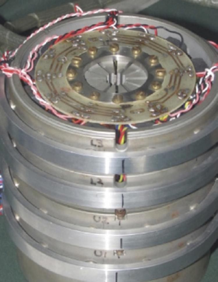
Fig. 2. The central part of the first STEM Cs corrector that improved the resolution of the microscope it was built into, with 6 multipole stages containing strong quadrupoles and octupoles, and 96 auxilliary coils for nulling parasitic aberrations. Corrector Ø ~ 12 cm.
The corrector (Fig. 2) is now displayed in a glass case in the Cavendish Lab, next to Deltrap’s proof-of-principle quadrupole-octupole corrector, and not far from the Cavendish’s crown jewels that include the apparatus with which J.J. Thompson discovered the electron in 1897, and the DNA model built by Watson and Crick in 1953.

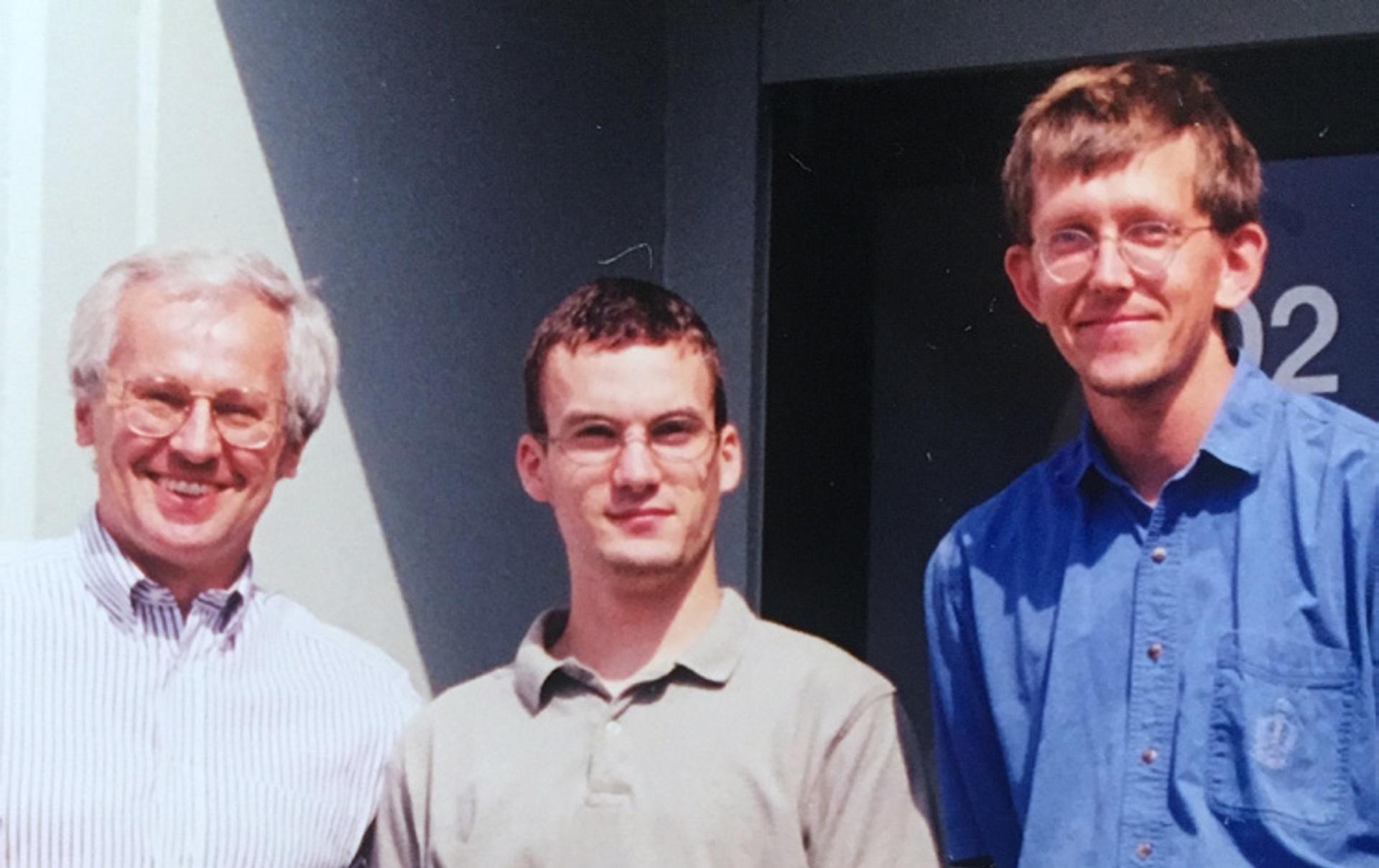
Fig. 3. Ondrej Krivanek, George Corbin and Niklas Dellby in front of Nion I building, which featured a large garage that we later converted into a mechanical assembly room. Nion can therefore claim that its origins were in the proverbial garage.
We made a really good microscope
The new microscope produced spectacular images of 2D materials such as graphene and of 1D materials such as nanotubes. We got into this field with samples provided by Valeria Nicolosi of TCD in Ireland, and by Kazu Suenaga of AIST Japan. Niklas and I brought these samples to Oak Ridge National Laboratory (ORNL), where we worked over a long weekend on the fourth electron microscope Nion had delivered to a customer. The popular wisdom back then was that the imaging technique we were using – high angle annular dark field (HAADF) imaging – could not usefully image light atoms such as carbon. The signal was supposed to be too weak to make the imaging of single atoms possible. Contrary to that “wisdom”, we started getting spectacularly clear images of nanotubes and graphene at a primary energy of 60 keV, which avoided heavy damage to the samples.
"I had many hours of operating other electron microscopes under my belt, but I had never seen images as clear as the ones I was getting from the Nion instrument."
I am not one given to exclamations, but I remember pausing, pushing my chair back from the control table, and proclaiming: “Niklas, we made a [really] good microscope!”

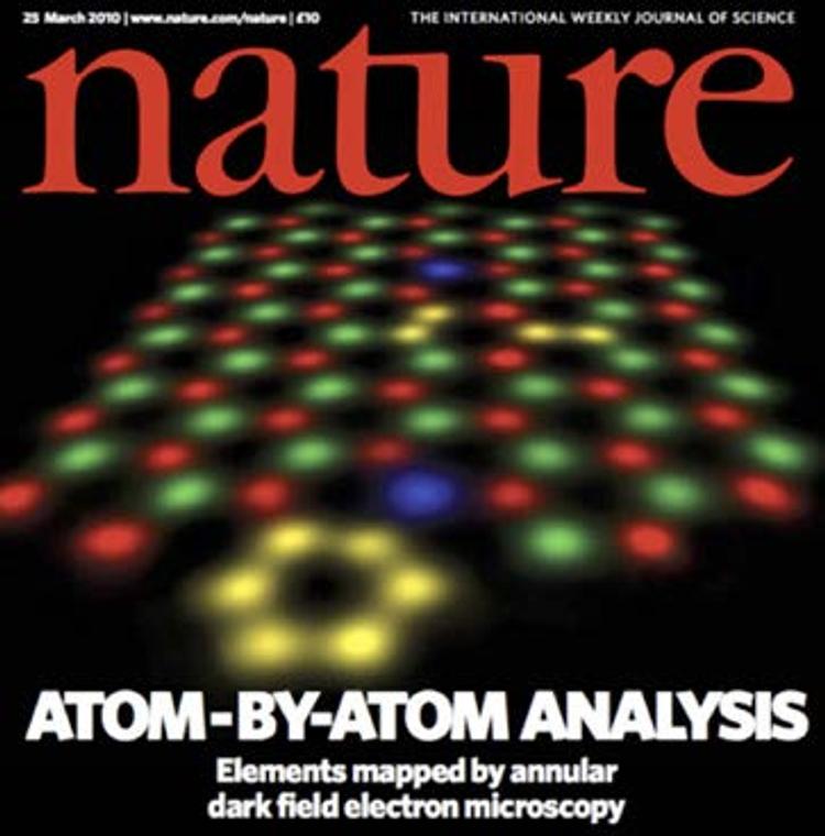
Fig. 4. Cover of the March 25, 2010 issue of Nature. It shows a medium angle annular dark field (MAADF) STEM image of monolayer BN with atomic substitutions. The experimental image was colorized to correspond to the types of atoms that were identified using image intensities, and rendered in a perspective view.
I was not the only one who thought so. Juan Carlos Idrobo, post-doc at ORNL at that time, walked into the lab one evening, and when he saw the results we were getting, he watched for a long time, as though glued to the spot. He and others began to do similar experiments at ORNL soon after, and a few months later, Matt Chisholm produced an iconic image of a BN monolayer with atomic substitutions that was featured on the cover of Nature (Fig. 4). Results obtained at ORNL later showed how a structure consisting of 6 silicon atoms anchored in a graphene sheet jumped back and forth between two quasi-stable configurations. EEL spectra with revealing fine structure features were obtained from single Si atoms embedded in graphene, at roughly the same time at ORNL and at the Daresbury SuperSTEM lab, semiconducting MoS2 nanowires were sculpted from a 2D MoS2 sheet also at ORNL, and a research group at the University of Vienna was able to “drive” a single Si atom in chosen directions in a graphene sheet by the electron beam.The increase in the available beam current allowed the elemental composition of materials to be efficiently mapped at atomic resolution both by EELS and by energy-dispersive X-ray spectroscopy (EDXS), precisely as we had expected.
Bonding information can be mapped too, using chemical shifts in EEL spectra of different elements (Fig. 5). All these capabilities amount to just a small fraction of the different kinds of research enabled by Nion’s aberration-corrected STEMs. There are now over 20 of these instruments in the world, and about 1000 aberration-corrected STEMs made by other manufacturers. It is no longer possible to cover all the creative work that’s being done with these instruments in a single monograph.

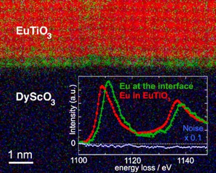
Fig. 5. EELS map of Eu atoms in EuTiO3 crystal leading to an atomically sharp interface with DyScO3. The intensity of each pixel in the map shows the Eu concentration worked out from a spectrum acquired at that pixel, the colour whether the atoms were 3+Eu (green) or 2+Eu (red). Insert shows Eu M4,5 edge threshold peaks from the interface (green) and away from it (red), with chemical shift of 2.5 eV due to the change in the Eu valence. L. Kourkoutis, D.A. Muller et al., proceedings IMC17 (Rio de Janeiro, 2010).
Major developments
Nion’s incredibly capable team, led by Niklas Dellby, Tracy Lovejoy, Chris Meyer, George Corbin, and myself, has done many amazing things. Aberration correction is now an established technique of electron microscopy, and we have focused on two new directions: developing flexible and user-friendly open-source software for imaging and analysis, and improving the energy resolution of electron energy loss spectroscopy.
Our software effort augments the advances made by aberration correction, making the instruments more powerful and user-friendly. The improved energy resolution would not have been possible without aberration correction: the monochromator and the electron energy loss spectrometer we have developed both use design principles we first introduced for aberration correction. The optical properties and unsurpassed stabilities of these instruments have pushed the energy resolution of EELS to 3 meV (100x energy resolution improvement relative to an electron microscope not using a monochromator), and 5 meV is attainable on a routine basis. This resolution level allows vibrational spectroscopy to be performed in the electron microscope, and it has opened up major new research areas: 0.2-2 nm spatial resolution imaging of phonons, including acoustic ones, and their interaction with crystal defects; the ability to detect and map hydrogen distributions; distinguishing different isotopes (Fig. 6); and damage-free analysis of organic and biological samples.

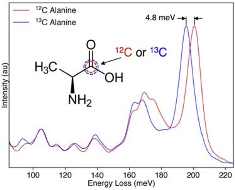
Fig. 6. Experimental vibrational spectra of two forms of the amino acid L-alanine, differing by a single 12C atom substituted by 13C. The 4.8 meV shift of the large peak at ~200 meV, due to the stretch of the C=O bond, can be mapped to reveal where the two types of molecules reside, at about 100 nm spatial resolution. J. Hachtel et al., Science 363 (2019) 525–528.
Bumps in the road for new projects
The ability to analyse the vibrational signature of biological samples without significant damage in the electron microscope is especially exciting. It relies on the fact that at the vibrational energies that we study (20-500 meV), the dipole interaction that excites optical phonons is delocalized, and it is possible to excite molecular vibrations in sample areas 30-100 nm or even further away from the electron beam. The energy that can be transferred to the sample by each fast electron is typically limited to < 1eV when the beam is that far away, and there is no significant radiation damage. The spatial resolution is not as good as when the electron beam is brought onto the sample and non-dipole signals are utilized, but a technique that can probe what molecules are present where in frozen hydrated biological samples at 30-100 nm resolution should still have plenty of important uses.
I was pursuing this idea in a research stay in Christoph Koch’s group at Humboldt University in Berlin, collaborating with Christoph, Benedikt Haas, Zdravko Kochovski, and Johannes Müller at HU, and Tracy Lovejoy, Niklas Dellby and Andreas Mittelberger at Nion. We had put together all the needed instrumentation and were about to start on experiments when the coronavirus pandemic hit, and I decided to return to Washington State.We plan to resume the work as soon as the pandemic allows.
A grateful scientist
Instrumentation developments resemble probing an uncharted territory, similar to the way the American Pacific Northwest was explored by Alexander Mackenzie and David Thompson over 200 years ago. Best guesses as to what welcoming lands may lie in which direction are followed by the long slog of an expedition, with day-to-day ingenuity in overcoming hardships and obstacles making the difference between failure and success. All the explorers contribute their utmost, and random encounters sometimes bring critical pushes in the right directions. I am deeply thankful to my co-explorers at Nion and in the labs we collaborate with for their incredibly fruitful efforts (Fig. 7).

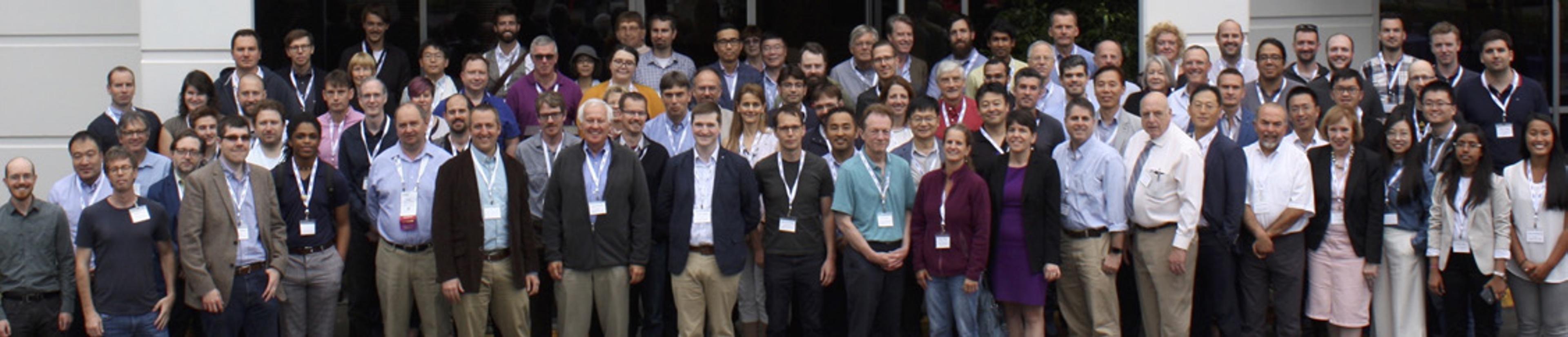
Fig. 7. August 2019 Nion Open House group photo showing the Nion team including Niklas Dellby, Tracy Lovejoy, Chris Meyer, George Corbin, Russ Hayner, Matt Hoffman, Peter Hrncirik, Nils Johnson, Josh Kas, Ben Plotkin-Swing, Lemek Robinson, Zoltan Szilagyi, Dylan Taylor, Janet Willis and Ondrej Krivanek, and Nion collaborators: Toshi Aoki, Nabil Bassim, Phil Batson, Andrew Bleloch, Wouter van den Broek, Peter Crozier, Christian Dwyer, Meiken Falke, Jordan Hachtel, Fredrik Hage, Bethany Hudak, Juan Carlos Idrobo, Demie Kepaptsoglou, Jani Kotakoski, Richard Leapman, Andy Lupini, Alan Maigne, Clemens Mangler, Molly McCartney, David Muller, Matt Murfitt, Xiaoqing Pan, Luca Piazza, Quentin Ramasse, David Smith, Rhonda Stroud, Toma Susi, Luiz Tizei, Kartik Venkatraman, Wu Zhou and many others
I am especially grateful to Niklas Dellby, with whom we founded Nion, and with whom I have enjoyed working together for nearly 30 years. Without his brilliance and hard work, the progress described here would not have been possible. What a voyage it has been!

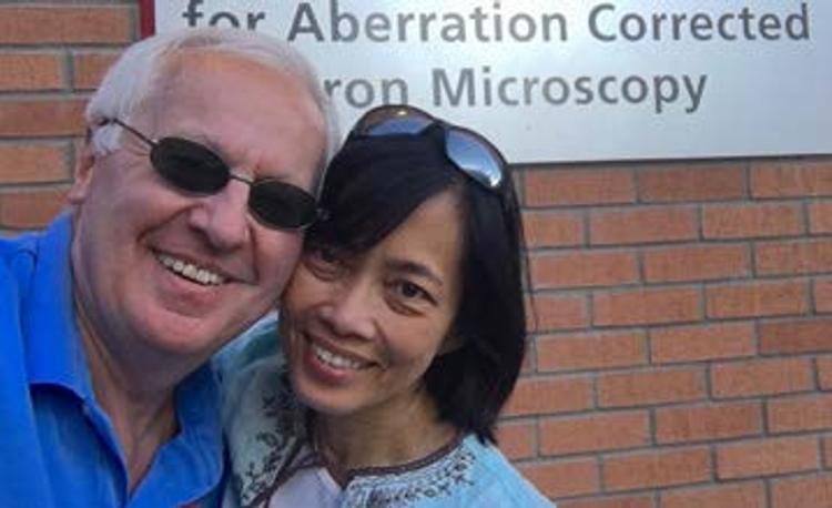
Fig. 8. Eda Lacar and Ondrej Krivanek in front of Arizona State University’s Southwestern Center for Aberration-Corrected Electron Microscopy. The center houses three aberration-corrected electron microscopes and plays a world-leading role in nanocharacterization.
Extended explorations are not easy on those we love, and it is their caring and support that allow us to go on. I thank my daughters Michelle and Astrid, and my nephew David for their love and understanding, and I am deeply grateful to Eda Lacar (Fig. 8) for her love and support. She expands my horizons in many wonderful and unexpected ways, and makes me into a better person.