


Not Even the Sky is the Limit
As told by Christoph Gerber
I was born in May 1942 in Basel, Switzerland, right in the middle of World War II, when Europe found itself in the biggest turmoil of its history. Remarkably, Switzerland could stay out of it. However, the risk to be drawn into it was always there, and people were of course pretty scared of it. We used to live very close to the French and German borders, and I vaguely remember an incident when in 1945 the American and allies forces made their attempt to cross the river Rhine north of Basel to enter Germany. Day and night one could hear the thunder of the artillery and the sky turned deep red when night fell. It must have made a deep impression on me because it seems it was one of the earliest incidences in my life that I can remember.

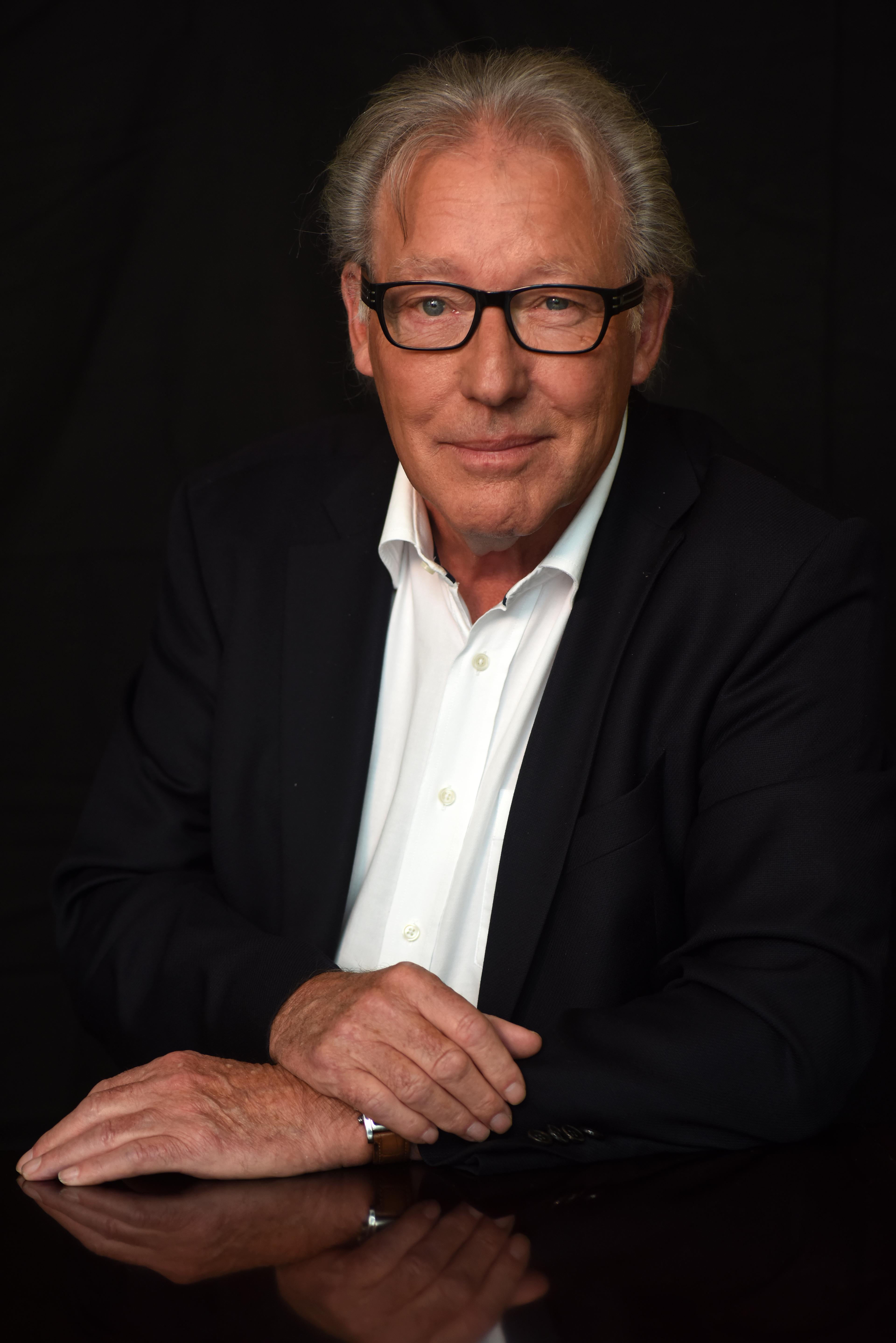
Christoph Gerber (Photo: Peter Bagde).
Quite early in my life I was already engaged with medical science – well, rather with the science of the dead, since my father was working in the pathology department of the University hospital in Basel. In spite of the fact that he was on the administrative side, we quickly learned such things that when people run a fever, mostly its cause is either a viral or bacterial infection. I also learned that little bugs living in your body getting out of hands are responsible for it. These were interesting lectures, and as children we were listening in awe to my father’s explanations regarding the human body and its function. Even more interesting, and leaving a great impression on me, was an exhibition in the pathology department showing all kinds of human parts preserved in display glass cabinets. However, getting used to this environment we were playing hide and seek among this cabinets. My favoured place to hide was behind a complete human skeleton in front of a black curtain. I knew that my younger sister never dared coming close.
Detour
In spite of all this scientific environment I have grown up with I took a detour to find a life in science. Known as a dreamer, after school, where I did not show a great deal of interest and therefore was a mediocre performer, I went through a mechanical engineering education, which eventually brought me to Stockholm in a managing position for a Swiss company working in military defence. I eventually was awarded a PhD from the University of Basel in physics, but this was in the future then.
In 1966 I joined the IBM research lab, where science fell upon me and changed my life forever. I teamed up with the late Heinrich Rohrer, Heini for people who knew him well. I am deeply grateful for all I have learned, and Heini was an extraordinary charismatic man, easy and fun to work with, and a great teacher. We all miss him deeply as a natural leader, a visionary, a stimulating scientist and a wonderful person.
Antiferromagnets
At that time, we began working on antiferromagnets called gadolinium aluminate (GdAIO3). Antiferromagnetism is a type of magnetic ordering that vanishes at a certain temperature. This took us into the field of critical phenomena and eventually led to crucial findings on magnetic phase transitions. K. Alex Müller a (co-)recipient of the Nobel Prize 1987, was then the head of physical Science at the IBM lab and had already pioneered the field of structural phase transitions. So slowly we established a world renowned reputation in critical phenomena. During that time, I led the project when Heini was on sabbatical at the University in Santa Barbara, CA, and it earned me the first of the many research awards that followed at the IBM lab.
During these early times at the IBM lab, a young crystallographer working on his master thesis joined the Lab. Georg Bednorz from the University of Münster basically took over the crystal growing lab, and showed people how to grow crystals like never done before. His master piece, a Strontium-titanate (SrTIO3) crystal, was the first worldwide and very much to the liking of Alex Müller who used it in his studies. The perovskite structure of the crystal triggered years later high Tc Superconductivity and eventually earned the pair a Nobel prize, but this was in the future then.
Scanning Tunneling Microscope
Towards the end of the seventies the interest shifted to the complex structure of surfaces, because the semiconductor industry was rapidly approaching the design of circuits on the nanoscale and not many tools were available to study the structure and properties of materials on this scale length. So when Gerd Binnig joined the lab at the end of the seventies, he and Heini started to contemplate a new device. The outcome, the Scanning Tunneling Microscope, a device working below the optical diffraction limit, took care of a quantum phenomenon called tunneling by guiding a tip over a conductive surface in the regime, where electron wavefunctions overlap, causing a current to flow from the foremost atom of the tip into the surface. Keeping the current constant allows to image surfaces on the atomic scale. The enormous resolution of the device was based on the exponential distance dependence of the tunnel current. Moving the tip perpendicular back and forth by the diameter of a single atom made the current change by a factor of thousand. People first had difficulties to believe that it was possible to position a tip in such close proximity of a surface. However the breakthrough came in 1983 with an experimental observation of one of the most intriguing phenomena in surface science at that time: atom by atom imaging of the 7x7 surface reconstruction in silicon Si(111) Thus, for the first time, it was possible to get up close and personal with individual atoms in a three dimensional representation.
At the beginning the project was considered high risk, so I was working on it for more than a year on my own, basically “under cover” until we got a feel how to overcome the tremendous problems like establishing the tip in the tunnel regime and taking care of vibration isolation etc.

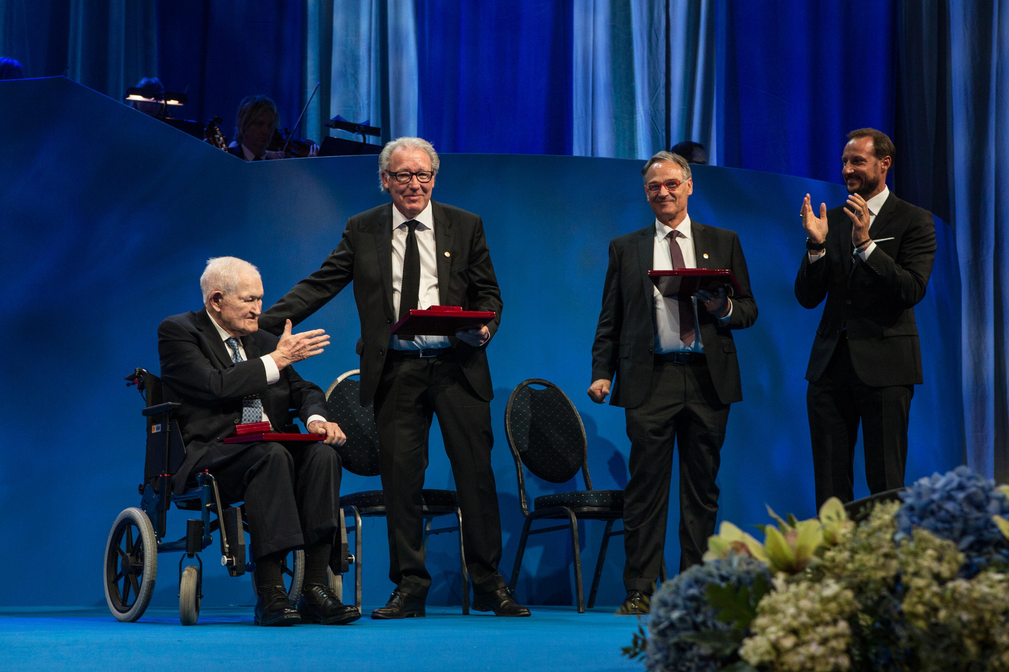
The three nanoscience laureates on stage at the ceremony in Oslo with their awards; from left: Calvin Quate, Christoph Gerber, Gerd Binnig and His Royal Highness Crown Prince Haakon (Photo credit: Thomas Brun, NTB Scanpix)
Ten stimulating years
I worked with Gerd roughly for the next ten years to come. They undoubtedly belong to the most inspiring, stimulating years of my life. Apart from what we basically call a genius (I am very serious), Gerd is a keen violin player, has designed unsinkable sailing boats and was very quick in picking up all kinds of sports. He introduced his own style of skiing and golf, and he was a brilliant forward in our football (soccer) team. We had a great time together and had lots of fun.
A high time at the IBM lab
It took the small, but steadily growing, community another two years to verify the initial results obtained at the IBM lab in Zurich, and it was only at a workshop at Oberlech in the Austrian Alps in 1985 that researchers started to realize the potential of the new method, as scientists verified the initial results obtained at the IBM two years earlier. Devices such as the atomic force microscope (AFM) have their roots in this meeting: in particular in a talk given by John Pethica from Cambridge University saying that in such close proximity between tip and sample a whole conglomerate of atomic forces must act on the tip. Weeks later this eventually triggered the idea of the atomic force microscope. However, during the last night of the workshop, the Alps were buzzing with crazy new ideas for using such microscopes in many different areas of science and technology. People were eager to get back to their labs and start working right away, although some almost missed the bus to the airport the next morning because they were still caught up in the discussions. Everyone present realized that something very special had happened: we were witnessing the beginning of nanoscience. A year later, in 1986, Gerd Binnig and Heinrich Rohrer shared the Nobel Prize in Physics “for their design of the scanning tunneling microscope”. Another year later Georg Bednorz and K.A. Müller followed waving the IBM flag. It indeed was high time at the IBM research lab.
The STM took scientists into uncharted territory by offering the ability to image surfaces in 3D at the atomic scale, but it only can image electrically conductive surfaces. So the question was how to image molecular and atomic details on non-conductive surfaces. At that time in the mid-eighties Gerd and I were on sabbatical leave in Cal Quate’s group at Stanford University and at the IBM lab in Almaden. One of my tasks was to help people at the west coast of the US to turn on the green light in operating their home built STMs at different universities such as Caltech, UCLA, Berkley, Stanford, and IBM. Of particular importance: the University of Santa Barbara in Paul Hansma’s group. Paul was one of the first believers of the new technology and one of the participants in that seminal Austrian workshop. He also was instrumental in transferring AFM technology towards application and commercialization within only five years after it was developed. However, this was in the future then.
A few weeks after that workshop, Gerd came up with the idea that it might be possible to measure these interactive forces with a microcantilever. We did a rough calculation and realized that for achieving atomic resolution on a non-conducting surface we needed to be able to detect forces at the level of 10^(-10) or even 10^(-11) newton!

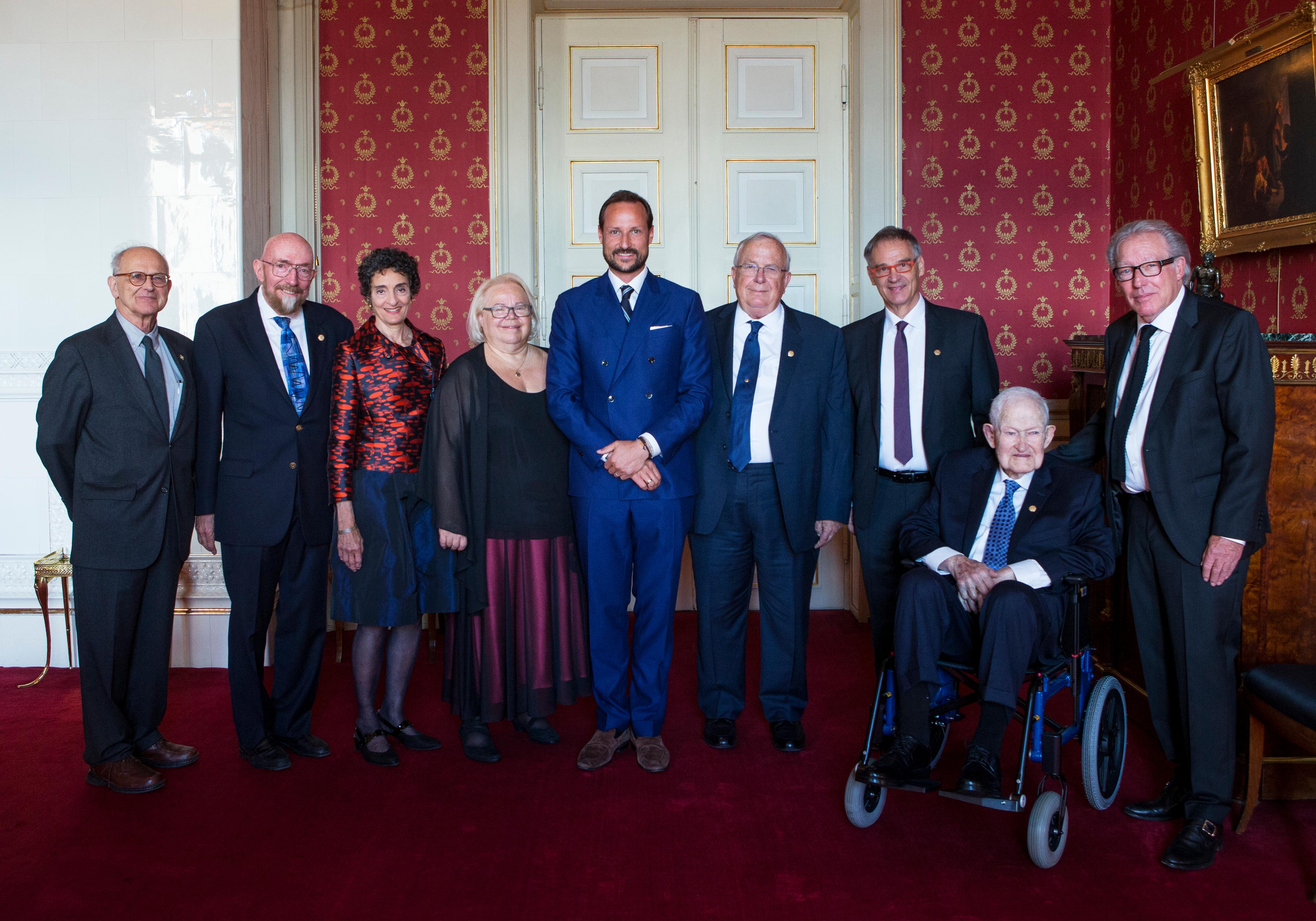
Christoph with all the other 2016 Kavli Prize laureates together with His Royal Highness Crown Prince Haakon at the prize ceremony in Oslo. From left Rainer Waiss, Kip S. Thorne, Carla J. Shatz, Eve Marder, His Royal Highness Crown Prince Haakon, Michael M. Merzenich, Gerd Binnig, Calvin Quate and Christoph Gerber (Photo credit: Thomas Eckhoff).
Turned down
I started to design a configuration of the first system. The heart of the device was a very thin gold foil just a few micrometers thick used as a cantilever, because cantilevers were of course not commercially available then. We took a fragment of a crushed diamond obtained from a stylus of a record player and glued it on to the cantilever foil to serve as a tip. Since the STM can measure displacements of 10^(-4) Angstroms, it was the obvious choice to measure the tiny forces that deflected the cantilever. Within five months, we had a working system. We did not get atomic resolution straight away on an Aluminum oxide surface, but we were close to submit a manuscript to Physical Review Letters, PRL, called ‘The Atomic Force Microscope’. One of the reviewers mentioned we could not call it Atomic Force Microscope since it does not show atomic resolution. We insisted that we will achieve atomic resolution. I personally believe, the editor in chief did not dare turning it down as it happened to our first STM manuscript sent to PRL, where reviewers’ arguments were that vacuum tunneling is already well known, and in spite of considering the work a technical jewel the manuscript should be rejected or to be left to the editor decision… The STM paper demonstrating the exponential behaviour of the tunnel current was turned down by the editor in chief, and so we published it in Applied Physics Letters.
As for the query of one of the reviewers concerning the AFM paper: within a year we had a more advanced instrument based on a batch-fabricated silicon cantilever produced by Tom Albrecht in Cal Quate’s group that showed atomic resolution for the first time on a graphite surface. Cal’s group were a stimulating bunch of youngsters to work with. Many of them e.g Dan Rugar are pillars in AFM technology and instrumental for the future developments in academia and industry.
However today this first AFM paper is the most cited experimental work published in Physical Review Letters.
Hole in one
These first results with the AFM on an Aluminum oxide surface were achieved during a long night exercise sometime in October 1985. Stanford has a great golf course, where e.g. the career of Tiger Woods started, but that was in the future then. Gerd and I stepped out of the lab 6 o’clock in the morning onto the first elevated tee overlooking the awakening silicon valley, already an industrial powerhouse back then, and I remembered that allegedly the double Nobel laureate John Bardeen, a keen golfer, mentioning that the hole in one in golf he made in his life meant more to him than his two Nobel prizes. In that game there was no hole in one for us. In fact is was so terrible that we lost all the balls we had and therefore we never got on to the 18th hole.
At that time, we could simply not foresee the dynamic in the development of the new technology we started. The sole idea for the AFM was actually getting atomic resolution on non-conducting surfaces. However, people have picked on this simple idea to scratch a surface with a cantilever and getting all kinds of very interesting scientific answers to questions on the atomic scale on surfaces and beyond. The STM shows the electronic state of matter on the atomic scale, but the AFM reveals the internal structure of atoms and molecules and has surpassed the STM to a great extent.
Powerful and versatile toolkit
Nature is the best example of a system functioning on the nanometer scale, where the involved materials, energy consumption and data handling are optimized. The emergence of the AFM in the then fledgling field of nanotechnology led to a shift of paradigm in the understanding and perception of matter at its most fundamental level. It undoubtedly has opened new avenues in physics, chemistry, biology and medicine and still is inspiring researchers around the world, testified so far by more than 350’000 scientific articles in peer reviewed journals (according to the web of science). The high flexibility of AFM to image, probe and manipulate materials with unprecedented resolution and the option to be combined with other technologies made it the most powerful and versatile toolkit in nanoscience and – technology – of today. As a consequence, new revolutionary concepts stimulated a number of new technologies for the benefit of mankind.
A long journey
In recent years we have taken AFM technology way beyond imaging and developed a diagnostic tool applicable in pushing the boundaries in personalized healthcare, developing arrays of cantilever as bio sensors. It all started in the mid-nineties where I was contemplating to develop a chemical AFM in order to get atomic and chemical resolution simultaneously on surfaces. Jim Gimzewski, a colleague and good friend at the IBM lab at that time, also a participant at this seminal workshop in Oberlech, was already famous to have taken the STM into various new directions, such as imaging single molecules and STM fabricated molecular superstructures at room temperature and much more. Together we were tinkering with the possibility to use just the surface of the AFM cantilever as a chemical sensor. Ernst Meyer, a physicist finishing his PhD in the group of Hans Güntherodt at the University of Basel, joined in. We published the outcome of this early work in two papers. It was the beginning of a long journey that began when I was still at the IBM lab full of hardship at times, but very interesting and in the end successful. I slowly turned into a sort of biologist also with the help of members of our group as we went along.
Turning into biology and medicine
Rüdiger Berger, a physics PhD student, Marko Baller, a chemist by training and physics PhD student, Hans Peter Lang, a physicist and later Jürgen Fritz, a bio physicist, indicated the direction of the interdisciplinary approach we anticipated to take the technology into biology and ultimately into medicine and diagnostics. Marko Baller led the way to develop a chemical nose in gaseous environment and Jürgen Fritz showed the possibility of the technology to be very specific and sensitive down to a single base mismatch on the DNA level in fluidic environment. Extending this work, Rachel McKendry, a chemist took it into multiple label free and quantitative detection of DNA binding, a second hint indicating that we were on the right track. Hans Peter Lang, also from the Güntherodt group at the University in Basel became my long standing collaborator for the developments that lay ahead of us and was instrumental in our achievements over almost the last two decades that followed.
In 2001 I retired from the IBM Lab and joined the NCCR National Center of Competence in nanoscience which I co-founded at the Institute of Physics at the University of Basel. We continued the work in taking on François Huber, a biochemist, Jiayun Zhang, a chemical physicist showed that we could monitor genes in their on and off state and basically revealing their malfunction. A very important result in view of the work that followed. Natalija Backmann, a protein specialist showing proteomics at work completed the team. Interactively we worked together with the group of Martin Hegner a biochemist who played an important role in many of the findings together with Thomas Braun and others.
In a series of publications over the years we could show our work has taken us either into the realm of personalized medical diagnostics on the genetic level by analyzing the BRAFV600E single-point mutation in total RNA extracted from surgical samples of metastatic melanoma. Showing that the method is faster than the standard Sanger or pyrosequencing methods and comparably sensitive as next-generation sequencing and that the processing time from biopsy to diagnosis is below one day and does not require PCR-amplification, sequencing and labels (work by François Huber). A different focus was on the diagnosis of patient health conditions before and after operations of malignant tumours monitoring the respiratory tract by non-invasive breath analysis (work by Hans Peter Lang). Many of these efforts could not have been achieved without the financial support of the Cleven foundation in Baar Switzerland. We are indeed enormously thankful for this.
When we started all this with Jim Gimzewski, now at UCLA Los Angeles, we never could foresee that we eventually would enter the clinic with this technology, but thanks to the inspiring contributions of all the researchers involved over the years we got there in the end.
Some of the researchers involved stayed in academia and became distinguished professors and others went in to Industry. Ernst Meyer is full professor at the Institute of Physics and the SNI at the University of Basel, Jürgen Fritz is professor at the Jacobs University Bremen, Martin Hegner is professor at CRANN in Dublin, Rachel McKendry is professor at UCL London, and Murali Ghatkesar is professor at TU Delft.

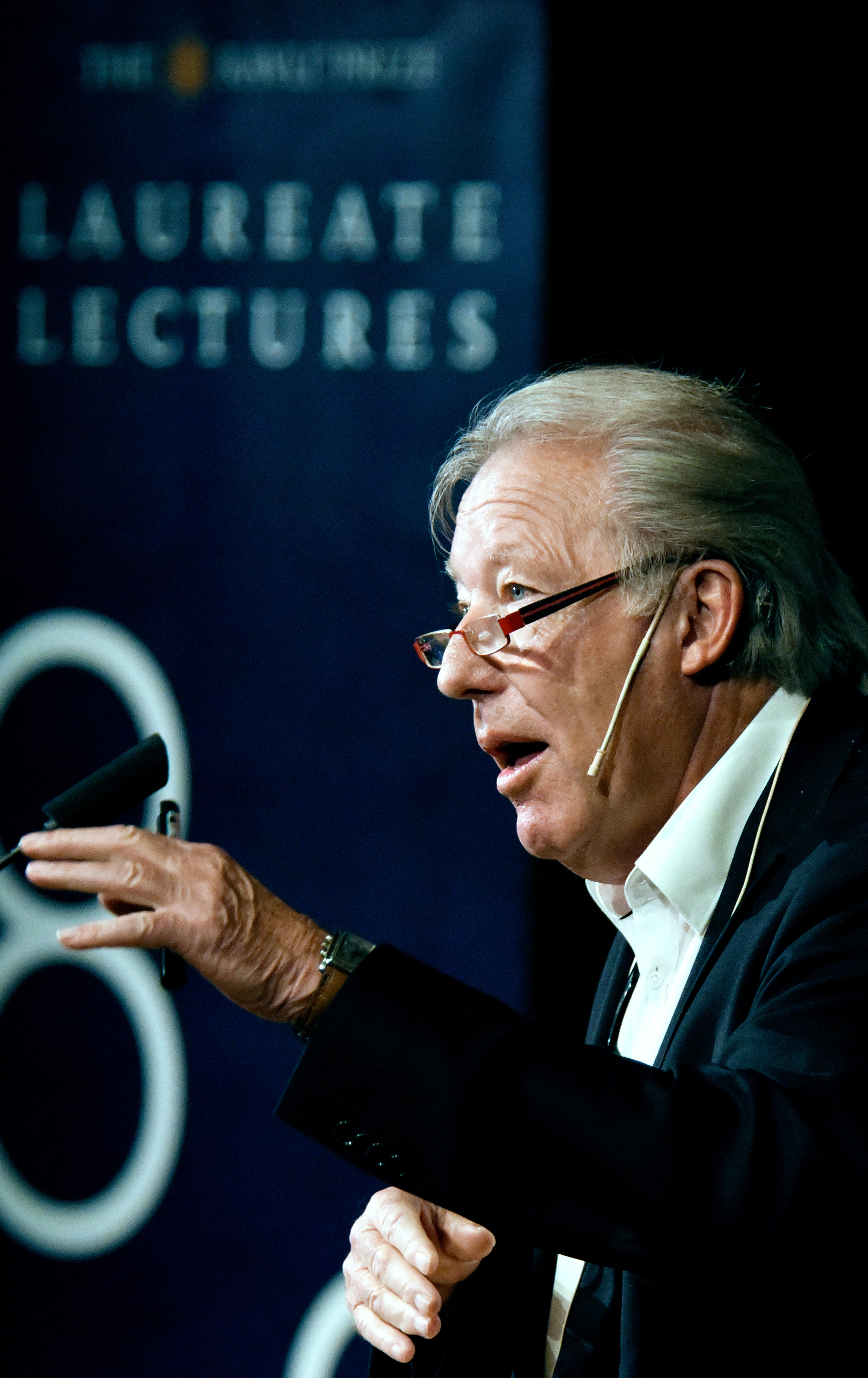
Christoph Gerber giving a lecture during the 2016 Kavli Prize week in Oslo (Photo credit: Thomas Eckhoff).
Nanoscience institute
Hans Güntherodt Institute of physics university Basel played a very important role in my career as a mentor and supporting my work all these years. His untimely passing in 2014 left a legacy in relentless promulgating nanoscience and in particular SPM technologies. He was one of the first people to appreciate the new technology of STM. He redirected his research as early as 1983 since he believed the technology could help to shine light on his research on amorphous metals to find structural evidence on the atomic scale which finally was achieved in Ernst Meyers group 30 years later. He has built up a center of excellence in STM and AFM research over the years at the University of Basel. Many of his PhD students are Professors or leading directors of institutes in nanoscience scattered all over the world. Because of the great knowledge accumulated in Güntherodt’s group I suggested to start a nanoscience institute at the University in Basel at the end of the nineties. The federal government granted our proposal based on an interdisciplinary effort involving people from quantum information all the way to life science and medicine. At that time, it was radically new and included a curriculum in nanoscience. When we started in 2001 Hans Güntherodt was the first director and it was the first institute of this kind worldwide. People did not believe that bringing together so many researchers from different disciplines with a common goal would ever work. Quite to the contrary after a few years it turned in to the now world renowned Swiss Nano institute SNI of today, successfully led by Christian Schönenberger. I still serve on the managing board of the SNI.
I have giving numerous plenary and invited talks throughout my career.
A great impression
One workshop left a great impression on me. The invitation came from Mark Welland Cambridge university, and also a participant of that seminal workshop in the Austrian Alps. The workshop in Cambridge was addressing new developments in AFM technology. However, what made it so exceptional was the place I stayed the night. It was in the flat of Paul Dirac the quantum genius of the last century at St. John college in Cambridge. The flat was overlooking a park where on the other side Charles Darwin use to be in residence. I was quite flattered.
All kinds of career developments
Mark is now the director of the Nano institute at Cambridge university, and he served as a Science advisor to the defence minister of the British government. He has been knighted by Queen Elisabeth; Sir Mark Welland. Other colleagues working with AFM followed suit. John Pethica Trinity college Dublin and Oxford university served as vice president of the Royal Society in London and also got a knighthood. Chun li Bai from Chinese Academy of Science started; I believe; with STM 1988 and is now the president of CAS and in this function the highest scientist in China. Flemming Besenbacher a virtuoso in SPM at the university of Aarhus in Denmark was elected chairman of the Carlsberg foundation and with this became a beer brewer. So AFM technology provided all kinds of interesting career developments.
A total surprise
Born and raised in Basel in the vicinity of my current working place at the SNI, I am still a curious person full of new ideas. I have met up with all kind of interesting, stimulating people and crazy characters from all walks of life that helped to shape my understanding of science and beyond. I feel enormously privileged to work in a profession that follows the arrow of time always engaged with the future. My life from where I was born and where I work today has come full circle. I am grateful for this and totally at ease. I am indeed very thankful that the Kavli Prize considered my contribution to science as worthy to be awarded as a co-recipient of this prestigious prize. It came as a total surprise.
As for the future of AFM, the original AFM is part of an exhibition at the Science Museum in London called “The making of the modern world”. The nearby Apollo capsule is therefore in good company because an AFM has already been sent to the Martian surface and one is currently on board the European Rosetta mission to investigate stardust on the nanoscale. It seems not even the sky is the limit for AFM technology.